

Sorry !!! This area is under construction.
Scanning Tunneling Microscopy/Spectroscopy (STM/STS)
in ambient conditions and in controlled atmosphere is developed in our
group during more than ten years. Few constructions of Scanning Tunneling
Microscopes/Spectroscopes (STM/STS) have been designed. STM/STS investigation
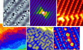
of the different samples including High Oriented Pyrolitical Graphite (HOPG),
Langmuir-Blodgette films (LB films), fullerens and carbon nanotubes, biological
molecules and membranes, and many others have been.
Ultra High Vacuum Scanning Tunneling Microscopy/Spectroscopy
are in progress in our group during five years. This techniques in combination
with traditional UHV investigation and sample preparation methods, such
as Low Energy Electron Diffraction , Auger Electron Spectroscopy (AES)
and Ion Spattering allow unique possibilities to investigate clean surfaces
of metals and semiconductors single crystals and different structures on
the surface.
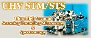
Ultra High Vacuum Scanning Tunneling Microscopy/Spectroscopy
(UHV STM/STS) are in progress in our group during five years. This techniques
in combination with traditional UHV investigation and sample preparation
methods, such as Low Energy Electron Diffraction (LEED), Auger Electron
Spectroscopy (AES) and Ion Spattering allow unique possibilities to investigate
clean surfaces of metals and semiconductors single crystals and different
structures on the surface.
Atomic Force Microscopy (AFM) and Scanning
Near Field Optical Microscopy (SNOM) which are developing in
our group are the powerful methods for the investigation of solid state
surfaces and the surface structures. AFM and SNOM techniques allow additional
unique possibilities and have some advantages in respect to the traditional
methods such as convenience Optical Microscopy or Scanning Electron Microscopy.
We are using our selfmaked modular Scanning Probe Microscope (SPM) which can work in both AFM and SNOM modes
to obtain information about the relief and the different properties of
the surfaces and the surface structures of the several samples with high
resolution up to the atomic scale.
Scanning Probe Microscope (SPM) which can work in both AFM and SNOM modes
to obtain information about the relief and the different properties of
the surfaces and the surface structures of the several samples with high
resolution up to the atomic scale.
|
 Scanning Probe Microscopes (SPM)